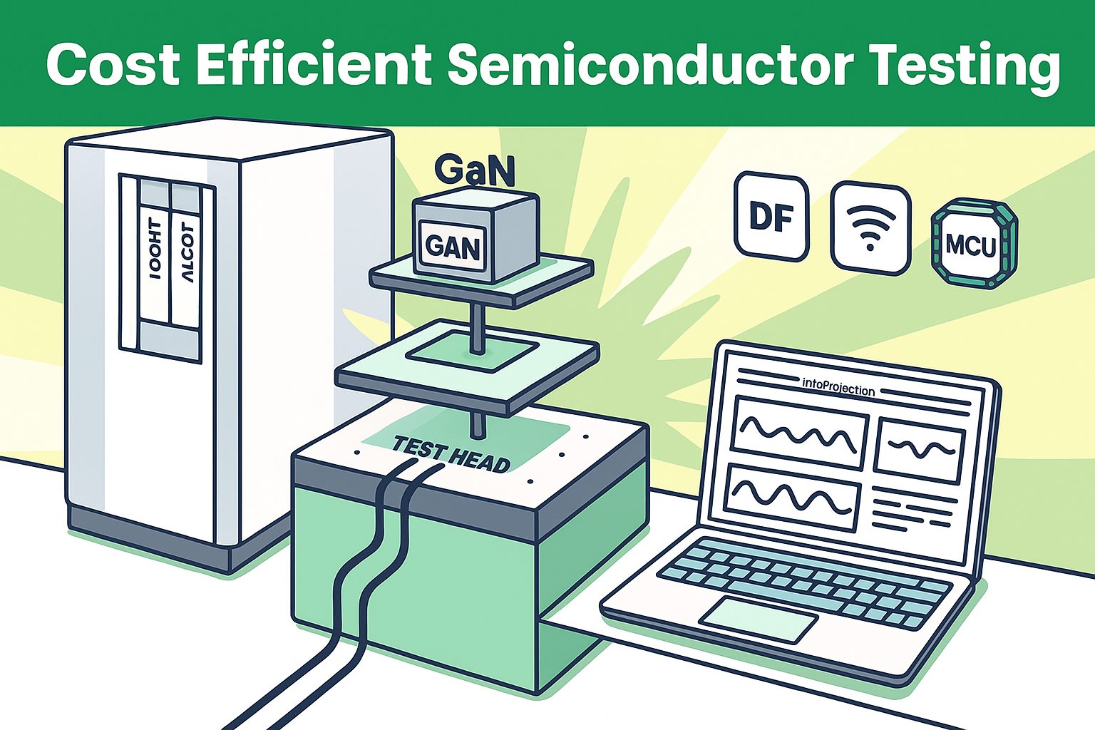
Designing for Efficiency: A Guide to Low Power VLSI Design – Part I
The need for a low power design
“Ever wonder why some devices last all day, while others don’t make it till lunch?”
The answer to the above question isn’t always about a bigger battery, it's also about designing a power efficient design. In an era where the usage of portable devices is increasing every second, power consumption is now not a design choice, it's a necessity.
This is where Low Power Design steps in—a combination of critical techniques aimed at reducing dynamic and static power consumption.
This article covers essential low power methodologies and strategies that design engineers can rely on for power optimization.
Components of Power Consumption
To first understand the concepts of how to reduce power consumption, we must understand what we, physical design engineers, mean by total power consumption.
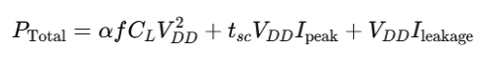
α activity factor (0 to 1)
f frequency
t_sc transition time
C_L capacitive load
V_DD supply voltage
I_leakage
leakage current
I_peak peak current
The total power consumption depends on dynamic and static power consumption
Dynamic power consumption depends on:
- Switching Power: The power consumption when a digital circuit changes from 0 to 1
- Short Circuit Power: This occurs when both pull-up and pull-down paths momentarily conduct during a signal transition (e.g., from 0 to 1)
Static power consumption comprises of Leakage Power (Power consumption when the transistor is ‘OFF’)
Running an Energy-Efficient Office Building
Imagine you’re managing a smart office building, and your goal is to reduce electricity bills.
Choosing Energy Smart Office Equipment: Multi VT
Option 1: High speed equipment
- These are top-of-the-line, super-fast machines.
- But they consume more power — even when idle, they draw some electricity (standby leakage).
- Example: A high-speed laser printer that warms up quickly and prints fast but uses a lot of standby power.
Option 2: Slower equipment
- These are energy-efficient devices.
- They’re a bit slower, but they use much less power, especially when not being actively used.
- Example: An inkjet printer that takes a few seconds to warm up but uses minimal power when idle
As a smart manager, you assign high speed equipment to teams which work in time critical projects and assign the rest to teams which work in less time critical projects.
What This Means for a Chip: This is the exact way, design engineers utilize multi VTs like LVT (faster but power hungry) and HVT (slower but power efficient) into critical and non-critical timing paths.
Smart fans in room: Clock Gating
Imagine you have a ceiling fan in a room that turns on automatically whenever someone is present and turns off when the room is empty.
- When the room is empty, the fan doesn’t spin — it saves electricity
- When someone enters, the fan starts spinning — providing comfort only when needed
- The fan only runs when there’s activity
What This Means for a Chip: The motion sensor is like a gating control — it decides whether to allow the fan to operate based on whether activity (someone entering the room) is needed.
If there’s no activity in that part of the chip, the clock is disabled, reducing dynamic power
Adjustable Room Lighting: Multi-Supply Voltage (MSV)
You install dimmer switches in different rooms.
- Bright meeting rooms need full lighting (high voltage).
- Hallways and storage areas only need dim lights (low voltage)
- Therefore, you save power by giving each room just the right amount of electricity it needs to function well.
What This Means for a Chip: MSV works by providing different parts of the chip with different voltages based on performance needs.
Unplugging unused office floors: Power Shut Off (PSO)
Imagine your company rents an entire 10-story building but only uses the first 5 floors regularly. The upper floors are only occupied once a month.
Rather than keeping lights, printers, and air conditioning running throughout the building, you installed main circuit breakers for the upper floors. When these floors aren’t in use, you cut the power completely.
You also implement smart systems that save computer data before shutdown and restore it when powered back on—ensuring no information is lost.
What This Means for a Chip:
- Entire sections (power domains) of a chip can be completely turned off when not needed
- Before powering down, smart systems are like retention flops that preserve essential data of the computers (flip flops)
- When power returns, the system resumes smoothly
PSO works like shutting off power to unused office floors—not just putting them on standby but completely powering them down to save maximum energy.
LP Techniques and their effect on the design
| Technique | Leakage Power | Dynamic Power | Timing Trade off | Area Trade off | Complexity | Design Considerations |
|---|---|---|---|---|---|---|
| Multi-Vt | 6X | 0% | 0% | 0% | Minimal | - Requires multi-Vt cell library |
| Clock Gating | 0% | 20% | 0% | <2% | Minimal |
- Requires clock-gating logic - Demands additional effort in static timing analysis |
| Multi-Supply Voltage (MSV) | 2X | 40-50% | 2% | <10% | Complex |
- Architecture and flow must be voltage domain aware - Requires multi voltage libraries and level shifters. - Increases verification complexity |
| Power Shut Off (PSO) | 10-50X | 0% | 4-8% | 5-15% | Complex |
- Requires switch insertion and validation - Requires isolation cell insertion and validation - Requires retention cell insertion and validation of retention control - Needs timing analysis during shutdown and wake-up - Includes restore logic validation - Increases verification complexity |
Power Intent File
Concepts like varying the flavors of VT cells and addition of clock gating can be easy as it relies on changing a few attributes in the PnR flow. But when it comes to more complex techniques like changing the voltage of domains and shutting off the power to parts of the circuit, how do we approach it? How do I define it in the flow?
The answer is a Unified Power Format file. The IEEE 1801 or the Unified Power Format file are defined as power intent files, that the EDA tools read in their flow to understand the details of the power domains, the power ports, the power nets, the isolation/level shifter/retention cells, the power switches etc.
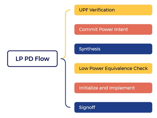
Physical Design Flow with LP Techniques
The Dynamic Development Journey of MSV and PSO Flow
A team of three engineers collaborated to develop the low power flow scripts, which can be seamlessly integrated into the standard place-and-route (PnR) flow using simple switches.
Power Intent Definition: Kickstarted the project by crafting a detailed power intent using Unified Power Format (UPF) to outline MSV domains and PSO regions.
Power Intent Verification: This process involves validating Power Intent Lint Errors, ensuring Power Intent alignment with RTL, and confirming implementable UPF, utilizing EDA tools like Conformal Low Power for efficient verification
Tool-Driven Synthesis: Leveraged Cadence Genus with the extended license, Genus Low Power Opt to develop a low power flow that can bind the domains with the libraries, commit the UPF and synthesize the design, ensuring addition of isolation and level shifter cells.
LP Equivalence Check: To ensure the design is maintaining accurate functionality during the stages of the flow, LEC check is mandatory. The comparison is extra important during the pre and post synthesis as RTL conversion to gate level netlist creates the most discrepancies. EDA tool Conformal Low Power can be utilized here also.
LP Implementation: The focus here is on streamlined UPF-driven flow. This process includes validating and initializing power domains, developing them with integrated power gates, and verifying the accurate insertion and domain-specific placement of LP cells. Additionally, secondary routing is confirmed for correctness, all supported by the Cadence Innovus Implementation System.
Signoff: The signoff phase emphasizes achieving design robustness through DRC and LVS signoff, RC extraction, and timing validation. This is complemented by static and dynamic power/rail analysis to ensure optimal power consumption The processes were supported by advanced EDA tools, Tempus Timing Signoff Solution, Voltus IC Power Integrity Solution, Quantas Extraction Solution, and Physical Verification System.
Strategic Insights
- Accurate analysis of low power design is a crucial step in ensuring power efficiency while meeting performance and functional reliability
- Ensure UPF accurately reflects the design intent to avoid verification errors
- Validate correct operation across all the active power states, ensuring no signal corruption or data loss
- Verify isolation and retention cell functionality to prevent data loss
- Place power switches (for PSO) and level shifters (for MSV) to minimize interconnect length and resistance
- Joules from Cadence can also help us get an insight in the early stage
- Dynamic Analysis and VCD files can help you get a better picture
- Activity profiling during dynamic analysis can help us analyze exact periods when there is high activity and analyze power at times when we are signaling the power gates to shutoff selected domains
- Verify that the power grid delivers stable voltages with acceptable IR drop (2 - 3 %)
- PSO wakeup can cause high in rush current, which can be solved by adding decoupling capacitors
- Timing paths involving level shifters and isolation cells are prone to violations, requiring up sized cells or buffers
- Analyze in-rush current and wake up latency during PSO wakeup
Unleash Powerful Results
As SOC Designers, we can opt for methods to help us enhance the effect of MSV and PSO techniques:
- Significant Voltage Scaling
- Techniques can be applied to a larger portion of the design
- MSV can be applied precisely to modules with high switching activity
- Both timing and power can be improved by optimizing voltage domain boundaries (reducing the number of ports that requires shifting and isolating)
- Usage of Multi VT/Sizes of Always on buffers, Isolation and Level shifter cells
- Fine grained selection of voltage domains in respect to critical and non-critical paths for MSV and PSO
A low-power design is crucial for creating energy efficient chips. Techniques like Multi-Supply Voltage (MSV) and Power Shut Off (PSO) significantly reduce power consumption but introduce challenges such as accurate and precise architecture planning, UPF verification, timing closure, and design complexity.
For deeper insight and to get assistance with the low-power VLSI design flow or its components, contact us at info@neural-semiconductor.com
 Faisal Adil Quadery, Engineer III